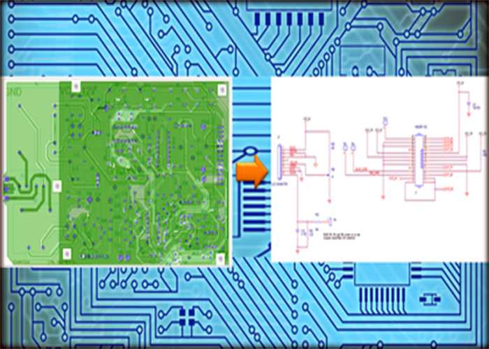
Reverse engineering is the art of disassembling an existing product into it’s component parts for the purpose of generating documentation aimed at re-manufacture of the product. As it applies to printed circuit boards in general, it is a process whereby a printed circuit board is stripped of all it’s components to reveal the board itself. Original design of the board can then be regenerated for the purpose of manufacturing additional boards.
This is particularly useful where the original manufacturer no longer produces or supports a given printed circuit board. There are many older, but very useful electronic products in service today where this may be true. In many instances it would actually be cheaper to generate the tools for fabricating new boards than it would be to replace the entire piece of equipment of which the circuit board is only a part.
Reverse Engineering of Printed Circuit Boards is one of our specialties. We can Scan (digitize) silver halide films, diazo films, transparencies, laser prints, pen plots, hand taped artwork, vellum, CAD drawings or actual Printed Circuit Boards. We can handle complex multi-layer cards with computerized net list generator and scanning process.
Capabilities:
- Layers: No limit (up to 6 layers, so far)
- of Pads: no limit
- Board size: no limit
- Components: Through hole, SMD or mixed including BGAs.
- Component sides: Single or both sided
What you receive:
- Schematic diagrams or Netlist.
- Bill of materials (BOM).
- Gerber files & NC drill file.
- Intelligent data base (on demand).
Our Reverse Engineering process allows a layout-driven design to back annotate PCB changes and additions to the schematic resulting improvements to old, obsolete designs. New chips can be replaced or added.
For fast quotation, please E-mail a digital photograph of the front and back of your card, along with approximate dimensions & number of layers. Please let us know what you need i.e. Schematic/Net list, Bill of material, Gerber files and/or a ‘clone’ of the card.
